We use cookies to enhance your experience. By continuing to browse this site you agree to our use of cookies. More info.
A team of researchers including a materials researcher from Oregon State University (OSU) has designed a superior tool to quantify light, contributing to a field called optical spectrometry that could enhance numerous things ranging from environmental monitoring to smartphone cameras.
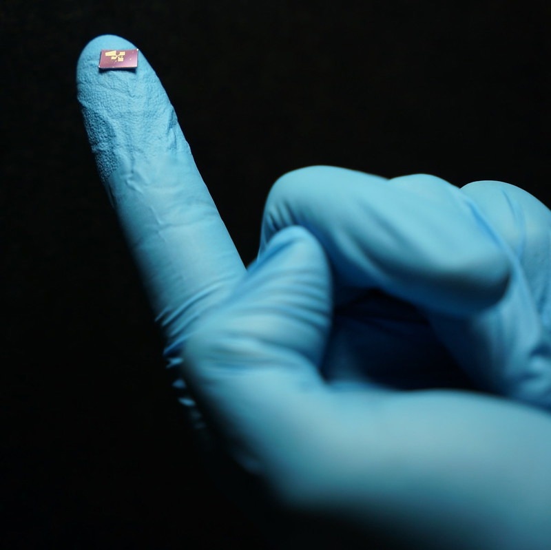
Spectrometer on a chip. Image Credit: Oregon State University
Guided by Finland’s Aalto University, the team built a robust, ultra-small spectrometer that can be positioned on a microchip and is worked using artificial intelligence (AI). Details of the novel spectrometer have been reported recently in the journal Science.
The study included a relatively new category of super-thin materials called two-dimensional (2D) semiconductors, and the result is a proof of concept for a spectrometer that could be easily integrated with a range of technologies—including security sensors, quality inspection platforms, space telescopes, and biomedical analyzers.
We’ve demonstrated a way of building spectrometers that are far more miniature than what is typically used today. Spectrometers measure the strength of light at different wavelengths and are super useful in lots of industries and all fields of science for identifying samples and characterizing materials.
Ethan Minot, Professor, Physics, College of Science, Oregon State University
Minot said that conventional spectrometers necessitate bulky mechanical and optical parts, whereas the new tool could be placed on the end of a human hair.
The new study proposes that those parts can be substituted with new semiconductor materials and AI, allowing spectrometers to be radically scaled down in size from the existing smallest ones, which are approximately the size of a grape.
Hoon Hahn Yoon from OSU led the study with colleague Zhipei Sun Yoon from Aalto University.
Our spectrometer does not require assembling separate optical and mechanical components or array designs to disperse and filter light. Moreover, it can achieve a high resolution comparable to benchtop systems but in a much smaller package.
Hoon Hahn Yoon, Study Lead, Oregon State University
The team expresses that the tool is 100% electrically governable concerning the colors of light it captures, which renders it huge potential for extensive usability and scalability.
“Integrating it directly into portable devices such as smartphones and drones could advance our daily lives,” Yoon said. “Imagine that the next generation of our smartphone cameras could be hyperspectral cameras.”
Those hyperspectral cameras could record and examine the information from visible wavelengths and allow for infrared imaging and examination.
“It’s exciting that our spectrometer opens up possibilities for all sorts of new everyday gadgets, and instruments to do new science as well,” Minot said.
In medicine, for instance, spectrometers are already being tested for their capability to detect minute variations in human tissue such as the difference between healthy tissue and tumors.
Likewise in the area of environmental monitoring, Minot added, spectrometers can precisely identify the type of pollution in the water, air, or ground, and the quantity.
It would be nice to have low-cost, portable spectrometers doing this work for us. And in the educational setting, the hands-on teaching of science concepts would be more effective with inexpensive, compact spectrometers.
Ethan Minot, Professor, Physics, College of Science, Oregon State University
Applications overflow as well for science-driven hobbyists, Minot stated.
If you’re into astronomy, you might be interested in measuring the spectrum of light that you collect with your telescope and having that information identify a star or planet. If geology is your hobby, you could identify gemstones by measuring the spectrum of light they absorb.
Ethan Minot, Professor, Physics, College of Science, Oregon State University
Minot believes that as research on 2D semiconductors advances, “we’ll be rapidly discovering new ways to use their novel optical and electronic properties.”
Exploration into 2D semiconductors has been sincerely performed for about 12 years, beginning with the investigation of graphene, a piece of carbon organized in a honeycomb lattice and measuring only the thickness of one atom.
“It’s really exciting,” Minot said. “I believe we’ll continue to have interesting breakthroughs by studying two-dimensional semiconductors.”
Besides Yoon, Minot, and Sun, the partnership included researchers from Zhejiang University, Shanghai Jiao Tong University, Yonsei University, Sichuan University, the University of Cambridge, and Aalto University.
The Academy of Finland supported this study.
Source: https://oregonstate.edu
Do you have a review, update or anything you would like to add to this news story?
Cancel reply to comment
The Thermo Scientific™ ARL™ EQUINOX 3000 X-ray Diffractometer for research enables accurate measurements.
KLA’s Filmetrics F40 allows you to transform your benchtop microscope into an instrument to measure thickness and refractive index.
This product profile describes the properties and applications of the ProMetric® I-SC Solution Imaging Colorimeter.
Davis Bowling
In this interview, AZoOptics talks to Davis Bowling, who provides guidance into extended reality (XR) optical testing and demonstrates how to optimize the testing process.
Jan Novotný
AZoOptics speaks to Jan Novotný, one of the founding members of Lightigo, about the significance of laser-induced breakdown spectroscopy (LIBS) in the elemental analysis field. Discussing Lightigo's rapid technology, Novotný discusses the latest trends in LIBS technology and its many benefits in several applications.
Dr. Stefan Weber
AZoOptics speaks to Phaseform, whose approach to adaptive optics is helping to refine optic technologies across applications like life sciences microscopy and optical inspection.
AZoOptics.com – An AZoNetwork Site
Owned and operated by AZoNetwork, © 2000-2022